Boundary Scan vs. Traditional ICT for BGA and Fine-Pitch Packages
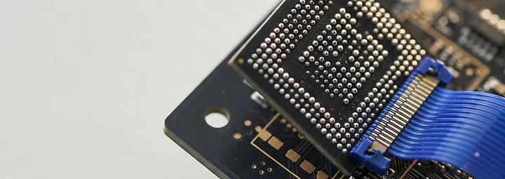
Every BGA hides its solder joints from a bed-of-nails probe. Here is exactly what ICT can still reach, what boundary scan adds, and where each one fails.
Boundary Scan vs. Traditional ICT for BGA and Fine-Pitch Packages
A ball grid array is, from a test engineer's point of view, a device that has deliberately hidden its own solder joints. The connections that matter most — the ones that fail in reflow — sit underneath the package where no probe can reach them.
This is the single most common reason a bed-of-nails fixture comes up short on a modern assembly. Understanding precisely what each technology can and cannot cover is what turns this from a religious argument into an engineering decision.
What a bed-of-nails fixture can actually reach
An ICT fixture contacts the board through test points on the accessible surface. For a BGA, that means:
- Outer ball rows are often reachable, depending on how much routing space the layout allows.
- Interior balls are not reachable at all. There is no path from the probe field to a ball under the package body.
- The nets those balls connect to are reachable elsewhere on the board, but testing the net does not test the solder joint. A continuity test from a via to a test point confirms the trace, not the ball.
This is the critical distinction. ICT can test the net. It cannot test the joint under the package. An open ball on an interior row can pass every ICT test on that net and still be a field failure.
What boundary scan adds
IEEE 1149.1 boundary scan embeds a shift register cell at each I/O pin of a compliant device. By driving one device's output cell and observing a connected device's input cell through the JTAG chain, you test the interconnect between them — through the package, through the ball, through the trace, and into the receiving device.
No probe is required. The device tests itself and its neighbours.
That makes boundary scan the only practical structural test for:
- Interior BGA ball joints
- Fine-pitch packages without accessible test points
- High-density assemblies where probe access was traded away for routing space
- Connectors and board-to-board interfaces
Where each one fails
ICT fails on: interior BGA joints, nets with no probe access, and any structure the fixture physically cannot reach. It also requires a mechanical fixture per design, which is a cost and lead-time constraint.
Boundary scan fails on: analog nets, power nets, devices that are not 1149.1 compliant, and — importantly — the interconnect between a compliant device and a non-compliant one. It also depends on chain integrity: a break in the scan chain takes out everything downstream. And it tests interconnect, not device function.
Neither technology covers memory devices, oscillators, or analog circuitry. Both leave those to functional test or built-in self-test.
A coverage comparison
| Failure mode | ICT | Boundary scan | |---|---|---| | Solder open, accessible net | Yes | Yes | | Solder open, interior BGA ball | No | Yes | | Solder bridge, accessible net | Yes | Yes | | Solder bridge, interior BGA ball | No | Yes | | Wrong component fitted | Yes | No | | Reversed / missing component | Yes | No | | Analog net integrity | Yes | No | | Passive value out of tolerance | Yes | No | | Powered functional behaviour | Partial | No |
The pattern is clear: the technologies are complementary, and the table shows why the argument over which one "wins" is misplaced. ICT is far better at component-level and analog faults. Boundary scan is the only option for the joints ICT cannot see.
The hybrid strategy most production lines land on
Run both, and let each do what it is good at.
- Boundary scan covers interconnect between compliant devices, prioritising BGA and fine-pitch areas.
- ICT covers component presence, orientation, value, and the analog and power nets boundary scan cannot touch.
- Functional test covers powered behaviour and the device-level functions neither structural method verifies.
Several boundary scan toolchains integrate directly with major ICT platforms, allowing both to run in a single pass on the same tester rather than as two separate operations. That integration is worth asking about early, because it changes the fixture requirements and the total cycle time.
Selection guidance
Use ICT alone when the board has good probe access, no BGA, and moderate density. A fixture is straightforward and coverage is strong.
Add boundary scan when the board has BGA or fine-pitch packages with inaccessible interior joints, when probe access is limited by routing density, or when a connector interface needs structural verification.
Consider boundary scan as the primary structural method when the assembly is dense enough that fixture access is impractical — though you will still need something for the analog and passive coverage boundary scan cannot provide.
Check chain integrity first. Before committing to a boundary scan strategy, confirm the devices you need are 1149.1 compliant and that the chain is intact and accessible. A single non-compliant device in the wrong place can break the topology you were counting on.
The question to ask at design review
Not "ICT or boundary scan," but: which nets have no probe access, and are the devices on either side of them compliant?
Answer that at layout time and the fixture problem largely solves itself. Answer it after tooling, and you are paying for a more complex fixture and still shipping with less coverage than you thought.
Browse JTAG boundary scan vendors covering IEEE 1149.1, 1149.6 and IJTAG 1687, or ICT service providers who build combined fixture and boundary scan programs.
Related in the directory: flying probe test providers, boundary-scan test providers, ICT program and software specialists and the full ICT vendor directory.